I’ve been working on a project where I need to drive a BLDC 3 phase HALL effect sensored motor.
I purchased a DRV8313EVM made by Texas Instruments. This board allows a user to connect a motor and make it move without having to construct their own circuit board.
The board has a USB port which connects a laptop to allow it to interface with the control software and utilises the inbuilt firmware. The software does not let you utilise the HALL sensors. This connection does not let you upload a custom firmware from CCS to the onboard MSP430G2553.
The documentation gives a partial instruction on how to upload a custom firmware using the SPI interface but it is not quite complete.
Connecting to MSP-EXP430G2
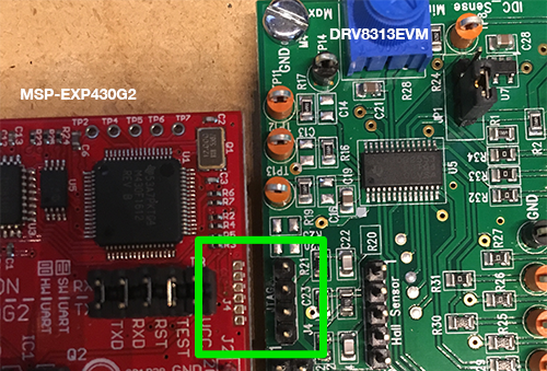
To upload a custom firmware you need to use a MSP-EXP430G2 and connect it from the JTAG interface labeled J4 on the EVM
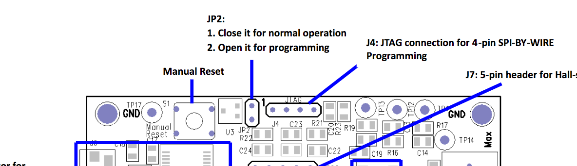
(Image sourced from DRV8313EVM user guide)
You need to connect 4 pins at J4 to the MSP-EXP430G2 and you need to open JP2 (remove the jumper).
The documents do not explain exactly how to do this so after a discussion on the TI community (an excellent resource by the way) I figured out how to do it with help.
You need to connect 4 pins to 4 of the pins on J4 of the MSP-430G2
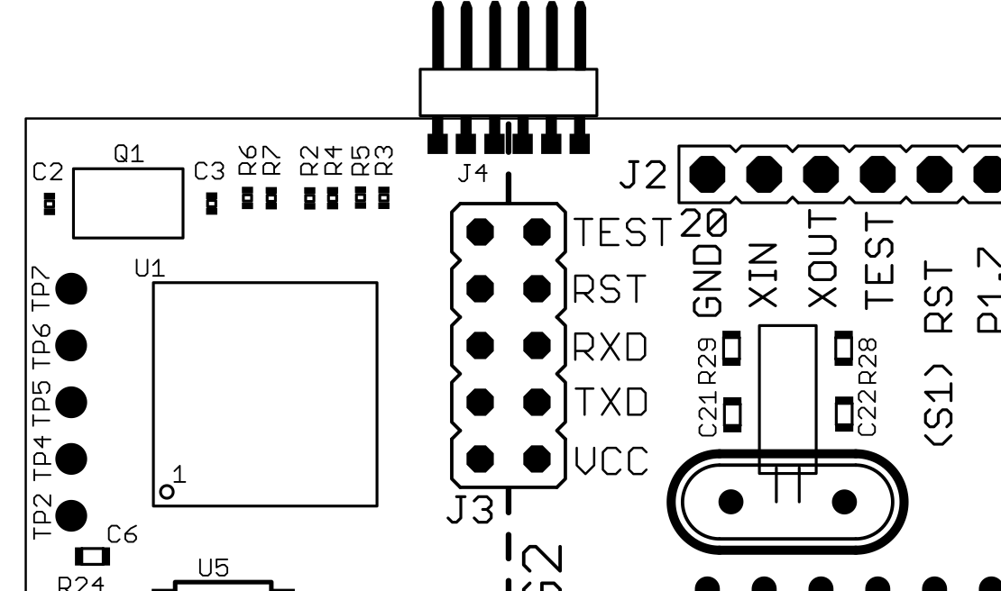
(Image sourced from the MSP-EXP430G2 Hardware Design Files (Rev. C))
There are 6 pins on the MSP but only 4 on J4 on the EVM.
The schematic shows the 4 pins and their labels. Since JP2 is removed the TLV809 is isolated.
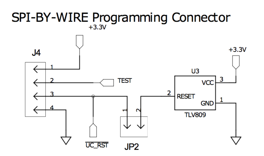
(Image sourced from the Hardware: DRV8313EVM file listed on this page)
|
PIN
|
LABEL
|
|
1
|
+3.3V
|
|
2
|
TEST
|
|
3
|
UC_RST
|
|
4
|
GND
|
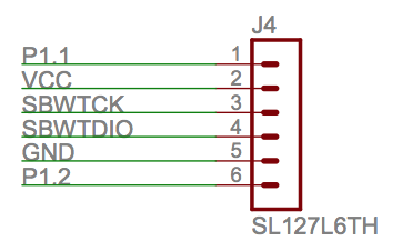
Unfortunately those labels do not match with the names of J4 on MSP-EXP schematic:
(Image sourced from the MSP-EXP430G2 Hardware Design Files (Rev. C))
We can quickly conclude that VCC is our 3.3V pin and that GND is pin 4 on the DRV8313EVM but we need to map the other 2.
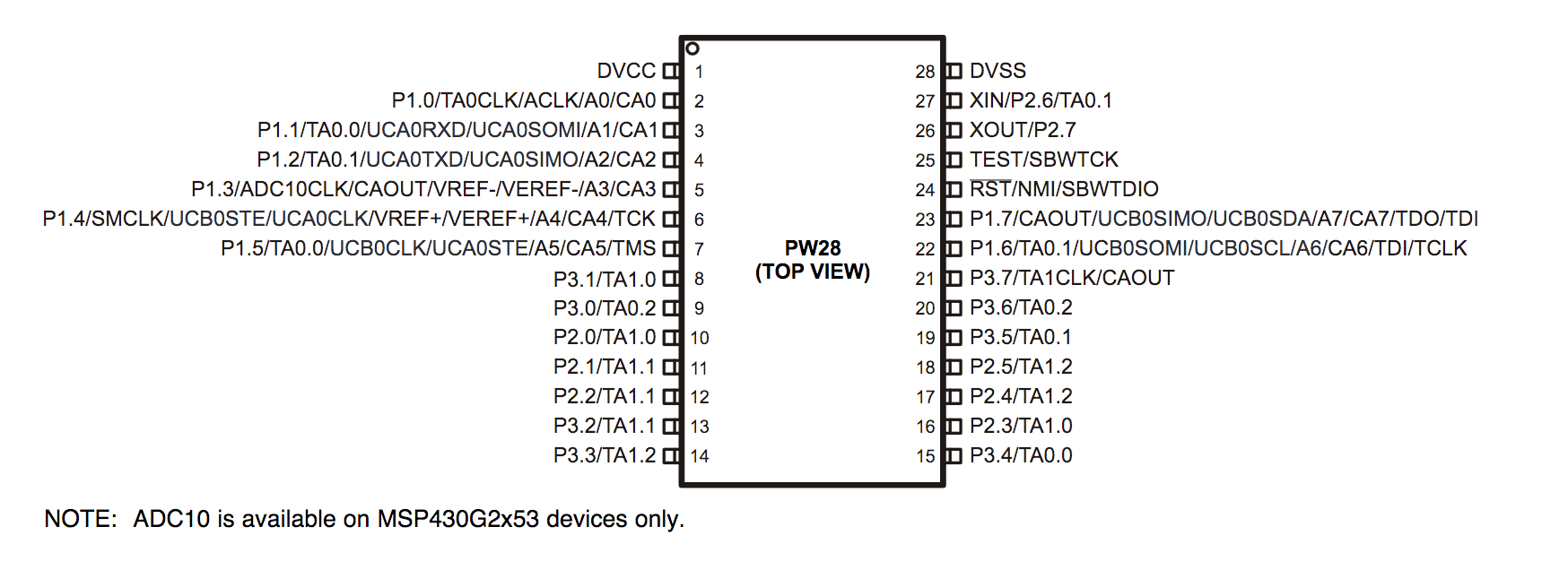
If we look at the PIN layout for for the MSP430G2553 we can see pin 25 and 24 are labelled as “TEST/SBWTCK” and “RST/NMI/SBWTDIO” so we can assume that on our DRV8313EVM PIN2 is “SBWTDIO” and PIN3 is “RST” (UC_RST and RST are the same although I am unsure what the meaning of UC is).
With that information we can get these pin mappings
|
DRV8313EVM J4 PINS
|
MSP-EXP430G2 PIN
|
|
N/A
|
1
|
|
1
|
2
|
|
2
|
3
|
|
3
|
4
|
|
4
|
5
|
|
N/A
|
6
|
It’s important to note that on the DRV8313EVM the pins run in a different order to the MSP-EXP430G2 pins. If you lay the 2 boards like in the image below on the MSP-EXP430G2 pin 1 is the top most pin, on the DRV8313EVM it is the bottom post pin.
The final connections should look like this
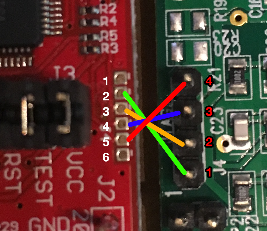
One additional note, you also need to rotate the RXD and TXD pins 90 degrees like in this image for the DRV8308EVM guide
You should now be able to apply power to the DRV8313EVM and see the PWR LED illuminate on the LaunchPad. From there you can connect to CCS and hit debug and it should work.
Notes
- This is my first time working any Texas Instruments platform so you should do your own verification on this, I don’t know if this information is applicable to any different versions of both boards.
- I used a Revision 1.5 LaunchPad
- Once you are done programming/debugging, reinstate JP2 so that the board will resume operation with your updated firmware
- Once the firmware is changed the USB connection and software become obsolete until you restore the default firmware
I’ve had such fun with this, it is something entirely new to me.